Samsung začel proizvajati 20 nm-bliskovni pomnilnik
Page 7
The Cost of Jumping to 40nm
The biggest issue with being a fabless semiconductor is that you have one more vendor to deal with when you're trying to get out a new product. On top of dealing with memory companies, component manufacturers and folks who have IP you need, you also have to deal with a third party that's going to actually make your chip. To make matters worse, every year or so, your foundry partner comes to you with a brand new process to use.
The pitch always goes the same way. This new process is usually a lot smaller, can run faster and uses less power. As with any company whose job it is to sell something, your foundry partner wants you to buy its latest and greatest as soon as possible. And as is usually the case in the PC industry, they want you to buy it before it's actually ready.
But have no fear. What normally happens is your foundry company will come to you with a list of design rules and hints. If you follow all of the guidelines, the foundry will guarantee that they can produce your chip and that it will work. In other words, do what we tell you to do, and your chip will yield.
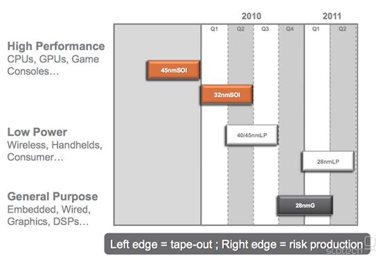
Global Foundries' 2010 - 2011 Manufacturing Roadmap
The problem is that if you follow every last one of these design rules and hints your chip won't be any faster than it was on the older manufacturing process. Your yield will be about the same but your cost will be higher since you'll bloat your design taking into account these "hints".
Generally between process nodes the size of the wafer doesn't change. We were at 200mm wafers for a while and now modern fabs use 300mm wafers. The transistor size does shrink however, so in theory you could fit more die on a wafer with each process shrink.
The problem is with any new process, the cost per wafer goes up. It's a new process, most likely more complex, and thus the wafer cost is higher. If the wafer costs are 50% higher, then you need to fit at least 50% more die on each wafer in order to break even with your costs on the old process. In reality you actually need to fit more than 50% die per wafer on the new process because yields usually suck at the start. But if you follow the foundry's guidelines to guarantee yield, you won't even be close to breaking even.
The end result is you get zero benefit from moving to the new process. That's not an option for anyone looking to actually use Moore's Law to their advantage. Definitely not for a GPU company.
The solution is to have some very smart people in your company that can take these design rules and hints the foundry provides, and figure out which ones can be ignored, and ways to work around the others. This is an area where ATI and NVIDIA differ greatly.
Zgodovina sprememb…
| Tema | Ogledi | Zadnje sporočilo | |
|---|---|---|---|
| Tema | Ogledi | Zadnje sporočilo | |
| » | Baterija 18650Oddelek: Elektrotehnika in elektronika | 10396 (3475) | FireSnake |
| » | Samsungov najprostornejši SSD s 15 TB že naprodaj (strani: 1 2 )Oddelek: Novice / Diski | 33132 (28715) | sodnicaN |
| » | Najprostornejši 2,5-palčni pogon na svetu je SSDOddelek: Novice / Diski | 11383 (8693) | Ghost7 |
| » | Samsung se odpoveduje proizvodnji trdih diskovOddelek: Novice / Nakupi / združitve / propadi | 9362 (7971) | Vanadium |
| » | Manjši trdi diski samsungOddelek: Kaj kupiti | 2597 (1795) | Glodko |